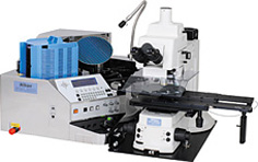
Nikon NWL200
Nikon’s newest and most sophisticated wafer loader for IC inspection microscopes.
The NWL200 series is the first lineup of wafer loaders for inspection microscopes capable of loading 100 micron thin wafers. Thanks to a new chuck system, the NWL200 series achieves highly reliable loading suitable for inspection of next-generation semiconductors. Improved wafer-sensing functions also help prevent damage to wafers, while wafer edge-chipping detection automatically detects edge-chipping defects.
Key Features | Specifications | Download Brochure